- 유관기관
- 전북대 산학협력단
- 서울대 반도체공동연구소
- 경북대 반도체공정교육센터
- 연구기관
- ETRI(한국전자동신연구원)
- 한국전기연구원
- 한국광기술원
- 나노종합기술원
- 한국나노기술원
- 관련정부부처 및 재단
- 교육부
- 과학기술정보통신부
- 정보통신산업진흥원
- 산업통상자원부
- 한국연구재단
- 한국산업기술평가관리원
Research Highlight
- Home
- TECHNOLOGY
- Research Highlight
2013~2016
-
2013
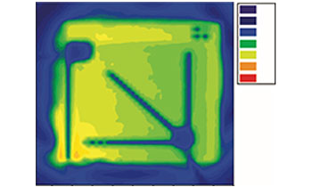
Improved heat dissipation in gallium nitride light-emitting diodes with embedded graphene oxide patternHan, N., Cuong, T. V., Han, M., Ryu, B. D., Chandramohan, S., Park, J. B., ... & Hong, C. H. (2013), Nature Communications, 4(1), 1-8.
The future of solid-state lighting relies on how the performance parameters will be improved further for developing high-brightness light-emitting diodes. Eventually, heat removal is becoming a crucial issue because the requirement of high brightness necessitates highoperating current densities that would trigger more joule heating. Here we demonstrate that the embedded graphene oxide in a gallium nitride light-emitting diode alleviates the selfheating issues by virtue of its heat-spreading ability and reducing the thermal boundary resistance. The fabrication process involves the generation of scalable graphene oxide microscale patterns on a sapphire substrate, followed by its thermal reduction and epitaxial lateral overgrowth of gallium nitride in a metal-organic chemical vapour deposition system under one-step process. The device with embedded graphene oxide outperforms its conventional counterpart by emitting bright light with relatively low-junction temperature and thermal resistance. This facile strategy may enable integration of large-scale graphene into practical devices for effective heat removal.
-
2014
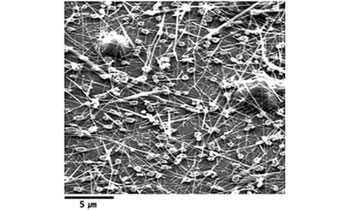
Growth of silicon nanowires in aqueous solution under atmospheric pressure.Park, N. M., & Choi, C. J. (2014), Nano Research, 7(6), 898-902.
A new method for growing silicon nanowires was presented. They were grown in an aqueous solution at a temperature of 85 ℃ under atmospheric pressure by using sodium methylsiliconate as a water - soluble silicon precursor. The structure, morphology, and composition of the as?grown nanowires were characterized by scanning electron microscopy, transmission electron microscopy, and energy dispersive X?ray spectrometry. It was also confirmed by X?ray powder diffraction and Raman spectroscopy that the silicon nanowire has hexagonal structure. It was possible to grow the crystalline silicon nanowires at low temperature under atmospheric pressure because potassium iodide, which was used as a gold etchant, sufficiently increased the surface energy and reactivity of gold as a metal catalyst with the Si precursors even at low temperature.
-
2016
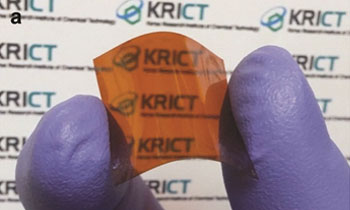
Wafer?scale, homogeneous MoS2 layers on plastic substrates for flexible visible?light photodetectorsLim, Y. R., Song, W., Han, J. K., Lee, Y. B., Kim, S. J., Myung, S., Lee, S. S., An, K. S., Choi, C. J., & Lim, J. (2016), Advanced Materials, 28(25), 5025-5030.
An appropriate solution is suggested for synthesizing wafer-scale, continuous, and stoichiometric MoS₂ layers with spatial homogeneity at the low temperature of 450 °C. It is also demonstrated that the MoS₂ -based visible-light photodetector arrays are both fabricated on 4 inch SiO₂/Si wafer and polyimide films, revealing 100% active devices with a narrow photocurrent distribution and excellent mechanical durability.